
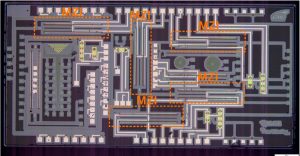
A Mach-Zehnder (MZI) Based Silicon Photonic Switch (Figure from [C24]).
Instructor: Prof. Mahdi Nikdast (E-mail: Mahdi.Nikdast@colostate.edu).
Office Hours (online): Friday; 11:00 AM to 12 PM. Check your Canvas for the Zoom call info.
Course Assistant: Amin Shafiee (E-mail: Amin.Shafiee@colostate.edu).
Course Assistant Office Hours: Wednesday; 4 PM to 5:30 PM. Check your Canvas for the Teams call info.
Lectures: Tuesday and Thursday, 3:30 PM to 4:45 PM in Rm. B4 (Engineering Building).
Lecture delivery: In person and online. If you are registered in the in-person session, then you MUST attend the lecture in person. If you cannot do so, please register for the online session of ECE544.
Course on Canvas: Click here
Course Summary
Why Silicon Photonics?
Silicon photonics is a rapidly growing field in communication (e.g., data centers, high-performance computing systems), computation (e.g., optical computing, photonic neural networks, AI accelerators), bio-sensing, Light Detection and Ranging (LIDAR) for autonomous driving, and in many other areas. Many companies are actively working and investing in silicon photonics (e.g., Intel, IBM, HPE, Facebook, Google, Microsoft, Global Foundries), addressing design and implementation challenges associated with this technology, paving the way to introduce this technology to the future systems in market. Meanwhile, many research groups in universities are studying silicon photonics, further pushing the application of this technology and addressing design, co-packaging, etc. challenges.
This course discusses the fundamentals and design principles of emerging silicon photonic integrated circuits and systems integrating such technology. This is a multidisciplinary course, where we discuss photonics, circuits, simulations, design automation and tools, design techniques, numerical methods, application of silicon photonics in high-performance computing, communication, etc. Topics related to design and analysis of fundamental silicon photonic devices as well as system architecture design and requirements will be discussed. In addition, the course will discuss advanced topics related to silicon photonic design requirements and challenges for emerging applications, such as neural networks and optical computing. Simulation tools from Synopsys will be used in the course. Would you like to be a part of this amazing journey? If so, then this is the course for you!
Course Learning Objectives
Here is a summary of ECE544 learning objectives:
- Learn fundamental concepts and operating principles of silicon photonic devices and circuits.
- Evaluate, analyze, and design primary passive and active silicon photonic devices.
- Evaluate, analyze, and design passive and active silicon photonic integrated circuits and interconnects.
- Work with Synopsys photonic tools and simulations and Klayout for chip layout design and verification.
- Explore applications of silicon photonics in high-performance computing systems and data centers, while studying various performance metrics, design challenges, and opportunities.
- Explore testing integrated photonic chips.
Course Textbook and Materials
- Instructor will introduce and discuss some Research Papers during the lectures;
- [TXT1] Lukas Chrostowski, Michael Hochberg, “Silicon Photonics Design: From Devices to Systems,” ISBN-13: 978-1107085459, ISBN-10: 1107085454, Cambridge University Press 2015. (main textbook)
Other useful/OPTIONAL references:
- [TXT2] Amnon Yariv, Pochi Yeh, “Photonics: Optical Electronics in Modern Communications,” 6th Edition, ISBN-13: 978-0195179460, ISBN-10: 0195179463, Oxford 2007.
- [TXT3] Michael J. Flynn, Wayne Luk, “Computer System Design: System-on-Chip,” ISBN: 978-1-118-00991-8, Wiley 2011.
- [TXT4] Mahdi Nikdast, Gabriela Nicolescu, Sebastien Le Beux, and Jiang Xu, “Photonic Interconnects for Computing Systems,” ISBN-13: 978-8793519800, ISBN-10: 879351980X, River Publishers, 2017.
- [TXT5] Ahmadreza Farsaei, “Introduction to Layout Design and Automation of Photonic Integrated Circuits,” Springer, 2023 (Link to access through CSU).
Grading Policy
| Homework Assignments | 20% |
| Lab Assignments | 35% |
| Course Project | Total: 45%
Weekly project reports: 10% Midterm project proposal and presentation: 15% Final project report and presentation: 20% |
The +/- grading scheme will be used, with the following scale
| >95% | 90 – 94% | 85 – 89% | 80 – 84% | 75 – 79% | 70 – 74% | 65 – 69% | 55 – 64% | 40 – 54% | <40% |
| A+ | A | A- | B+ | B | B- | C+ | C | D | F |
Homework and Lab Assignments Procedures, Submission Policy
Homework Assignments: To receive full credit for your homework, show all reasonable steps in solving problems. All the homework assignments should be uploaded electronically on Canvas.
Lab Assignments: Lab assignments are a very important component of this course. You will learn how to design and simulate silicon photonic components and devices, and by the end of the semester, will be able to design more sophisticated circuits. We use a set of simulation tools from Synopsys. After the first two to three labs, you will become comfortable with the tools and will be on your way to designing some interesting devices/circuits. Synopsys webpage is a good resource to learn the tools. Similar to homework assignments, lab reports should be uploaded electronically on Canvas.
In addition to simulation-based labs, we will work with some equipment from Keysight to learn how to test integrated photonic chips. For these labs, we will provide detailed instructions and you should answer some questions that will be given to you for each lab. Your report for the experimental labs should include a short summary of the lab and how you setup the equipment, any observations, and answers to the questions.
Late Submission Policy: Late homework will not be accepted unless the lateness is due to circumstances beyond your control (proof is required). To receive full credit, lab reports must be turned in on the date due. Late lab reports will be accepted, but points will be deducted from the score (-5 per day).
Instructions to submit your files: All the submitted files should be in PDF format and submitted electronically on Canvas. Make sure the submission is successful and readable.
Important information for students:
All students are expected and required to report any COVID-19 symptoms to the university immediately, as well as exposures or positive tests (even home tests).
- If you suspect you have symptoms, or if you know you have been exposed to a positive person or have tested positive for COVID (even with a home test), you are required to fill out the COVID Reporter (https://covid.colostate.edu/reporter/).
- If you know or believe you have been exposed, including living with someone known to be COVID positive, or are symptomatic, it is important for the health of yourself and others that you complete the online COVID Reporter. Do not ask your instructor to report for you.
- If you do not have internet access to fill out the online COVID-19 Reporter, please call (970) 491- 4600.
- You may also report concerns in your academic or living spaces regarding COVID exposures through the COVID Reporter. You will not be penalized in any way for reporting.
- When you complete the COVID Reporter for any reason, the CSU Public Health Office is notified. Students who report symptoms or a positive antigen test through the COVID Reporter may be directed to get a PCR test through the CSU Health Network’s medical services for students.
For the latest information about the University’s COVID resources and information, please visit the CSU COVID-19 site: https://covid.colostate.edu/.
Academic Integrity
This course will adhere to the CSU Academic Integrity Policy as found in the General Catalog (http://www.conflictresolution.colostate.edu/academic-integrity) and the Student Conduct Code (http://www.conflictresolution.colostate.edu/conduct-code). At a minimum, violations will result in a grading penalty in this course and a report to the Office of Conflict Resolution and Student Conduct Services.
All submitted work should be your own. Copying of language, structure, images, ideas, or thoughts of another, and representing them as one’s own without proper acknowledgement (from web sites, books, papers, other students, solutions from previous offerings of this course, etc.) and failure to cite sources properly is not acceptable. Sources must always be appropriately referenced, whether the source is printed, electronic, or spoken. My policy is that of zero tolerance. Minor first infraction in HWs and presentations will lead to a zero score as well as one letter level (e.g. A to B) reduction in the course grade. Project or Major or repeated infractions in HWs and presentations will result in “F” grade for the course as well as reporting to the Dean’s Office.
Diversity Statement
As the instructor in ECE544, I am deeply committed to helping build an inclusive culture in this classroom, in the Department of Electrical and Computer Engineering, in the Walter Scott, Jr. College of Engineering, and at CSU. Each individual brings diversity to our class in the identities they hold, the ways they think, their interests and skills, their background and past experiences. To me, inclusion means not only accepting these differences, but embracing them and understanding that we can leverage these differences to be better engineers.
My goal for this class is to create an environment where we do not discriminate against individuals because of their identities (e.g., race, ethnicity, sex, gender identity, sexual orientation, religion, nationality, age, levels of ability). It is also important to understand that even when we hold egalitarian beliefs, we can hold implicit or unconscious biases that can also influence the way we treat others or approach engineering design. It is my expectation that students in this class will:
- Adhere to the CSU Principles of Community https://diversity.colostate.edu/principles-of-community/;
- Work in teams in ways that recognize the contributions of all team members and provide all team members the opportunity to learn;
- Examine their own behaviors and refrain from acting in biased ways;
- Reflect on the ways bias can influence engineering work;
- Speak with the professor when biased behaviors may occur from other students, their TAs, and the professor;
- Be sensitive to context and acknowledge that hurtful comments can sometimes be inadvertent but they still have an impact.
Topics (Dates/Topics may change with reasonable notice.)
| Week | Summary of Topics | Readings | HW | Lab |
| W1 (Aug. 21) | No Lectures! | |||
| W2 (Aug. 28) | Introduction to Silicon Photonics (Lec1, Lec2): Limitations of electrical interconnects, history of silicon photonics, primary building blocks of a silicon photonics link, applications of silicon photonics. | Chapters 1, 2
[1-9] |
HW1 | |
| W3 (Sep. 4) | Optical Waveguides I (Lec1, Lec2): Fundamental concepts and properties of silicon photonics waveguides, basics of guided waves, Silicon on Insulator (SOI) wafers, strip and rib waveguides. | Chapter 3, [10], Chapters 1 and 2 from [11] | ||
| W4 (Sep. 11) | Optical Waveguides II (Lec1, Lec2): Approximate methods to model optical waveguides (effective index method, Marcatili’s approach), numerical methods and simulations, MODE simulation. | Chapter 3 from [TXT1] and Chapter 3 from [TXT2], [12-15] | Lab 1 | |
| W5 (Sep. 18) | Optical Waveguides III (Lec1, Lec2): Waveguide loss, waveguide bends, Y-branches, splitters, fundamentals of interferometers. | Chapters 3 and 4 from [TXT1], [16] | ||
| W6 (Sep. 25) | Coupling Light into Chips (Lec1, Lec2): Fundamentals of edge coupling and vertical coupling, grating couplers, brag gratings. | Chapters 4 and 6 from [TXT1], [20-26] | ||
| W7 (Oct. 2) | Silicon Photonics Devices I (Lec1, Lec2): Mach-Zehnder Interferometers (MZIs), design, simulation and analysis. | Chapter 4 from [TXT1], [27-31] | ||
| W8 (Oct. 9) | Silicon Photonics Devices II (Lec1, Lec2): Miroring resonators (MRs), applications, design, simulation and analysis. | Chapters 4 and 6 from [TXT1], [32-42] | ||
| W9 (Oct. 16) | Silicon Photonics Devices III (Lec1, Lec2): Directional couplers, layout design and simulation of mircoring resonators, KLayout, layout design and optimization, KLayout, programmable design kits (PDKs). | Chapters 4 and 6 from [TXT1], [43-48] | ||
| W10 (Oct. 23) | Compact Models (Lec1, Lec2): Compact photonic models, circuit simulation and design using compact models. | Chapter 9 from [TXT1] and [49-52] | ||
| W11 (Oct. 30) | Silicon Photonics Interconnects for HPC Systems (Lec1, Lec2): Optical interconnects in manycore system, optical routers, communication protocols, performance. | [53-58]
[J9-J11], [J16] |
||
| W12 (Nov. 6) | Advanced Topics I (Lec1, Lec2): Optical loss and crosstalk in silicon photonics. | [J6], [J8], [J14], [J17], [J19], [C6], [C16], [59] | ||
| W13 (Nov. 13) | Advanced Topics II (Lec1, Lec2): Fabrication non-uniformity and design for manufacturability (DFM). | |||
| W14 (Nov. 20) | Fall Break (No Lectures!) | Chapter 11 and 12 from [TXT1], [61]-[66] | ||
| W15 (Nov. 27) | Advanced Topics III (Lec1, Lec2): Nanophotonics neural networks and AI photonic hardware accelerators. | [J20], [C20], [C21], [C25], [C26], [67]-[71] | ||
| W16 (Dec. 4) | Final Presentations |
References
[1] I. A. Young et al., “Optical I/O Technology for Tera-Scale Computing,” in IEEE Journal of Solid-State Circuits, vol. 45, no. 1, pp. 235-248, Jan. 2010.
[2] Interconnect Scaling, Prof. Krishna Saraswat (https://web.stanford.edu/class/ee311/NOTES/InterconnectScalingSlides.pdf)
[3] David Thomson, Aaron Zilkie, John E Bowers, Tin Komljenovic, Graham T Reed, Laurent Vivien, Delphine Marris-Morini, Eric Cassan, Léopold Virot, Jean-Marc Fédéli, Jean-Michel Hartmann, Jens H Schmid, Dan-Xia Xu, Frédéric Boeuf, Peter O’Brien, Goran Z Mashanovich and M Nedeljkovic, “Roadmap on Silicon Photonics,” in Journal of Optics, 2016.
[4] A. Narasimha et al., “A Fully Integrated 4× 10-Gb/s DWDM Optoelectronic Transceiver Implemented in a Standard 0.13 μm CMOS SOI Technology,” in IEEE Journal of Solid-State Circuits, vol. 42, no. 12, pp. 2736-2744, Dec. 2007.
[5] M. Hochberg et al., “Silicon Photonics: The Next Fabless Semiconductor Industry,” in IEEE Solid-State Circuits Magazine, vol. 5, no. 1, pp. 48-58, winter 2013.
[6] E. F. Anderson, A. Gazman, Z. Zhu, M. Hattink and K. Bergman, “Reconfigurable Silicon Photonic Platform for Memory Scalability and Disaggregation,” Optical Fiber Communications Conference and Exposition (OFC), San Diego, CA, 2018, pp. 1-3.
[7] Christopher V. Poulton, Ami Yaacobi, David B. Cole, Matthew J. Byrd, Manan Raval, Diedrik Vermeulen, and Michael R. Watts, “Coherent solid-state LIDAR with silicon photonic optical phased arrays,” Opt. Lett., 42, 4091-4094, 2017.
[8] Adrián Fernández Gavela, Daniel Grajales García, Jhonattan C. Ramirez and Laura M. Lechuga,”Last Advances in Silicon-Based Optical Biosensors,” in Sensors, 2016.
[9] Romy Fain, Felippe Barbosa, Jaime Cardenas and Michal Lipson, “Photonic Needles for Light Delivery in Deep Tissue-like Media,” in Nature Scientific Reports, 2017.
[10] Kurt E. Oughstun and Natalie A. Cartwright, “On the Lorentz-Lorenz formula and the Lorentz model of dielectric dispersion: addendum,” Opt. Express, 11, 2791-2792, 2003.
[11] Graham T. Reed and Andrew Knights, “Silicon Photonics: An Introduction”, Wiley Publishers.
[12] Yong Ma, Mee Koy Chin, and Seng-Tiong Ho, “An Iterative Method for the Analysis of Rectangular Waveguides with External Effective Index Correction,” SPIE, vol. 3552, 1998.
[13] Photonic Research Group, Ghent University, “Dielectric Waveguides”.
[14] D. V. Batrak and S. A. Plisyuk, “Applicability of the Effective Index Method
for Simulating Ridge Optical Waveguides,” Quantum Electronics, vol. 36, no. 4, pp. 349-352, 2006.
[15] W. J. Westerveld, S. M. Leinders, K. W. A. van Dongen, H. P. Urbach and M. Yousefi, “Extension of Marcatili’s Analytical Approach for Rectangular Silicon Optical Waveguides,” Journal of Lightwave Technology, vol. 30, no. 14, pp. 2388-2401, July, 2012.
[16] Tong Chen, Hansuek Lee, Jiang Li, and Kerry J. Vahala, “A general design algorithm for low optical loss adiabatic connections in waveguides,” Opt. Express 20, 22819-22829 (2012).
[17] Ruijun Wang, et al., “III–V-on-Silicon Photonic Integrated Circuits for Spectroscopic Sensing in the 2–4 μm Wavelength Range,” Sensors, vol. 17, no. 8, 2017.
[18] Sébastien Rumley, et al., “Optical Interconnects for Extreme Scale Computing Systems,” Journal on Parallel Computing, vol. 64, May 2017, Pages 65-80, 2017.
[19] S. Romero-García, Bin Shen, F. Merget and J. Witzens, “Packaged MZIs passively balanced by means of multimode grating couplers,” Photonics North (PN), Quebec City, QC, 2016, pp. 1-1.
[20] Chrostowski and Hochberg, Silicon Photonics Design: From Devices to Systems, 2015 – Chapter 5 “Optical I/O”
[21] David J. Lockwood and Lorenzo Pavesi, “Silicon Photonics II – Components and Integration,” 2011 – Chapter 3 Interfacing Silicon Nanophotonic Integrated Circuits and Single-Mode Optical Fibers with Diffraction Gratings
[22] Dirk Taillaert, PhD Thesis, “Grating Couplers as Interface between Optical Fibres and Nanophotonic Waveguides”, 2004, IMEC
[23] Oscar Yun Wang, MSc Thesis “Grating coupler design based on silicon-on-insulator”, 2013
[24] A. Mekis et al. “A Grating-Coupler-Enabled CMOS Photonics Platform,” IEEE Journal of Selected Topics in Quantum Electronics, 17.3 (2011), pp. 597–608. doi: 10.1109/JSTQE.2010.2086049
[25] Wang, Yun, Wang, Xu, Flueckiger, Jonas, Yun, Han, Shi, Wei, Bojko, Richard, Jaeger, Nicolas A. F., Chrostowski, Lukas, “Focusing sub-wavelength grating couplers with low back reflections for rapid prototyping of silicon photonic circuits”, Optics Express, vol. 22, no. 17: OSA, pp. 20652–20662, 08/2014
[26] Wang, Y., Yun, H., Lu, Z., Bojko, R., Shi, W., Wang, X., Flueckiger, J., Zhang, F., Caverley, M., Jaeger, N.A.F., Chrostowski, L., “Apodized Focusing Fully Etched Sub-wavelength Grating Couplers”, IEEE Photonics Journal, 04/2015
[27] P. Sun, R. M. Reano, “Submilliwatt thermo-optic switches using free-standing silicon-on-insulator strip waveguides”, Optics Express, Vol. 18 Issue 8, pp. 8406-8411 (2010).
[28] Yuya Shoji, Kenji Kintaka, Satoshi Suda, Hitoshi Kawashima, Toshifumi Hasama, and Hiroshi Ishikawa, “Low-crosstalk 2 × 2 thermo-optic switch with silicon wire waveguides,” Opt. Express 18, 9071-9075 (2010).
[29] D. Patel, V. Veerasubramanian, S. Ghosh, W. Shi, A. Samani, Q. Zhong, D. V. Plant, “A 4×4 fully non-blocking switch on SOI based on interferometric thermo-optic phase shifters”, Optical Interconnects Conference, 2014.
[30] David Patel, Venkat Veerasubramanian, Samir Ghosh, Alireza Samani, Qiuhang Zhong, and David V. Plant, “High-speed compact silicon photonic Michelson interferometric modulator,” Opt. Express 22, 26788-26802 (2014).
[31] Xiaoguang Tu, Tsung-Yang Liow, Junfeng Song, Xianshu Luo, Qing Fang, Mingbin Yu, and Guo-Qiang Lo, “50-Gb/s silicon optical modulator with traveling-wave electrodes,” Opt. Express 21, 12776-12782 (2013).
[32] B. E. Little, S. T. Chu, H. A. Haus, J. Foresi and J. -. Laine, “Microring resonator channel dropping filters,” Journal of Lightwave Technology, vol. 15, no. 6, pp. 998-1005, June 1997.
[33] Michal Lipson, “Guiding, Modulating, and Emitting Light on Silicon-Challenges and Opportunities,” J. Lightwave Technol. 23, 4222- (2005)
[34] W. Bogaerts et al., “Nanophotonic waveguides in silicon-on-insulator fabricated with CMOS technology,” in Journal of Lightwave Technology, vol. 23, no. 1, pp. 401-412, Jan. 2005.
[35] B. Jalali and S. Fathpour, “Silicon Photonics,” in Journal of Lightwave Technology, vol. 24, no. 12, pp. 4600-4615, Dec. 2006.
[36] W. Bogaerts*, P. De Heyn, T. Van Vaerenbergh, K. De Vos, S. Kumar Selvaraja, T. Claes, P. Dumon, P. Bienstman, D. Van Thourhout, R. Baets, “Silicon microring resonators”, Laser & Photonics Reviews, 2011.
[37] Shaoqi Feng, Ting Lei, Hui Chen, Hong Cai, Xianshu Luo, and Andrew W. Poon, “Silicon Photonics: from a microresonator perspectives,” Laser Photonics, vol. 6, no. 2, p. 145-177, 2012.
[38] Xiaokun Wang, Xiaowei Guan, Qiangsheng Huang, Jiajiu Zheng, Yaocheng Shi, and Daoxin Dai, “Suspended ultra-small disk resonator on silicon for optical sensing,” Opt. Lett. 38, 5405-5408 (2013).
[39] W. S. C. Chang, Principles of Optics for Engineers. Cambridge, U.K.: Cambridge Univ. Press, 2015.
[40] K. S. Chiang, Integrated Optic Waveguides. Hoboken, NJ, USA: Wiley, 2001.
[41] B. Lin and C. Lea, “Crosstalk Analysis for Microring Based Optical Interconnection Networks,” in Journal of Lightwave Technology, vol. 30, no. 15, pp. 2415-2420, Aug.1, 2012.
[42] Xuanqi Chen, Zhifei Wang, Yi-Shing Chang, Jiang Xu, et al., “A Comprehensive Electro-Optical Model for Silicon Photonic Switches,” IEEE Computer Society Annual Symposium on VLSI (ISVLSI), Hong Kong, July 2018 (IEEE TCVLSI Best Paper).
[43] H. Haus, W. Huang, S. Kawakami and N. Whitaker, “Coupled-mode theory of optical waveguides,” in Journal of Lightwave Technology, vol. 5, no. 1, pp. 16-23, January 1987.
[44] H. Haus, W. Huang, “Coupled-mode theory,” in Proceedings of the IEEE, vol. 79, no. 10, pp. 1505-1518, October 1991.
[45] Wei-Ping Huang, “Coupled-mode theory for optical waveguides: an overview,” J. Opt. Soc. Am. A 11, 963-983 (1994).
[46] A. Yariv, “Critical coupling and its control in optical waveguide-ring resonator systems,” in IEEE Photonics Technology Letters, vol. 14, no. 4, pp. 483-485, April 2002.
[47] Nirmalendu Acharyya and Gregory Kozyreff, “Multiple Critical Couplings and Sensing in a Microresonator-Waveguide System,” in Physics Review Applied, vol. 8, p. 034029, 2017.
[48] Gregory Kozyreff and Nirmalendu Acharyya, “Dispersion relations and bending losses of cylindrical and spherical shells, slabs, and slot waveguides,” Opt. Express 24, 28204-28220 (2016).
[49] Lukas Chrostowski, et al., “Design methodologies for silicon photonic integrated circuits”, Proc. SPIE , Photonics West, 2014.
[50] Z. Zhang et al., “Compact Modeling for Silicon Photonic Heterogeneously Integrated Circuits,” in Journal of Lightwave Technology, vol. 35, no. 14, pp. 2973-2980, 15 July15, 2017.
[51] Zeqin Lu, Jaspreet Jhoja, Jackson Klein, Xu Wang, Amy Liu, Jonas Flueckiger, James Pond, and Lukas Chrostowski, “Performance prediction for silicon photonics integrated circuits with layout-dependent correlated manufacturing variability,” Opt. Express 25, 9712-9733 (2017).
[52] W. Bogaerts and L. Chrostowski, “Silicon Photonics Circuit Design: Methods, Tools and Challenges,” in Laser and Photonics Review, vol. 12, no. 4, April 2018.
[53] R.G. Beausoleil, et al., “Nanoelectronicand NanophotonicInterconnect,” Proceedings of the IEEE, Feb. 2008.
[54] H. Gu, K. H. Mo, J. Xu and W. Zhang, “A Low-power Low-cost Optical Router for Optical Networks-on-Chip in Multiprocessor Systems-on-Chip,” IEEE Computer Society Annual Symposium on VLSI, Tampa, FL, 2009, pp. 19-24.
[55] R. Ji, J. Xu, L Yang, “Five-Port Optical Router Based on MicroringSwitches for Photonic Networks-on-Chip”, IEEE Photonics Technology Letters, March, 2013.
[56] Sébastien Le Beux, Jelena Trajkovic, Ian O’Connor, Gabriela Nicolescu, Guy Bois, et al., “Multi Optical Network-on-Chip for Large Scale MPSoC,” IEEE Embedded Systems Letters, Institute of Electrical and Electronics Engineers, 2010.
[57] D. Vantrease et al., “Corona: System Implications of Emerging Nanophotonic Technology,” International Symposium on Computer Architecture, Beijing, 2008, pp. 153-164.
[58] Y. Pan, J. Kim and G. Memik, “FlexiShare: Channel sharing for an energy-efficient nanophotonic crossbar,” International Symposium on High-Performance Computer Architecture, Bangalore, 2010, pp. 1-12.
[59] M. Bahadori, S. Rumley, D. Nikolova and K. Bergman, “Comprehensive Design Space Exploration of Silicon Photonic Interconnects,” Journal of Lightwave Technology, vol. 34, no. 12, pp. 2975-2987, 15 June15, 2016.
[60] W. Bogaerts, P. De Heyn, T. Van Vaerenbergh, K. De Vos, S. Kumar Selvaraja, T. Claes, P. Dumon, P. Bienstman, D. Van Thourhout, R. Baets, “Silicon microring resonators”, Laser & Photonics Reviews, 2011.
[61] W.A. Zortman, D.C. Trotter, and M.R. Watts. “Silicon photonics manufacturing”. Optics Express 18.23 (2010), pp. 23598–23607.
[62] X. Wang, W. Shi, H. Yun, S. Grist, N. A. F. Jaeger, L. Chrostowski, “Narrow-band waveguide Bragg gratings on SOI wafers with CMOS-compatible fabrication process”. Optics Express 20.14 (2012), 15547-58.
[63] N. Ayotte, N.; D.Simard, A.; LaRochelle, S., “Long integrated Bragg gratings for SOI wafer metrology,” Photonics Technology Letters, 2015.
[64] L. Chrostowski, et al., “Impact of Fabrication Non-Uniformity on Chip-Scale Silicon Photonic Integrated Circuits”, OFC 2014.
[65] X. Wang et al., “Lithography simulation for the fabrication of silicon photonic devices with deep-ultraviolet lithography,” The 9th International Conference on Group IV Photonics (GFP), San Diego, CA, 2012, pp. 288-290.
[66] Xu Wang, Yun Wang, Jonas Flueckiger, Richard Bojko, Amy Liu, Adam Reid, James Pond, Nicolas A. F. Jaeger, Lukas Chrostowski, “Precise control of the coupling coefficient through destructive interference in silicon waveguide Bragg gratings”, Optics Letters, vol. 39, issue 19, pp. 5519-5522, 10/2014.
[67] D. Woods, T. J. Naughton, “Photonics Neural Networks”, Nature Physics, vol. 8, 2012.
[68] Yichen Shen, Nicholas C. Harris, Scott Skirlo, Mihika Prabhu, Tom Baehr-Jones, Michael Hochberg, Xin Sun, Shijie Zhao, Hugo Larochelle, Dirk Englund and Marin Soljačić, “Deep Learning with Coherent Nanophotonic Circuits,” Nature Photonics, vol. 11, 2017.
[69] J. Mower et al., “High-fidelity quantum state evolution in imperfect photonic integrated circuits,” Physical Reviews A, 92, 032322, 2015.
[70] Carolan Jacques et al., “Universal Linear Optics,” Silence 349.6249, 2015, pp. 711-716.
[71] V. Sze, Y. Chen, T. Yang and J. S. Emer, “Efficient Processing of Deep Neural Networks: A Tutorial and Survey,” Proceedings of the IEEE, vol. 105, no. 12, pp. 2295-2329, Dec. 2017.
Course Sponsor