
The NGPV Center at CSU performs cutting edge research in partnership with industry leading companies. Started in 1991, the lab has been at the forefront of CdTe solar PV research since 1991.
Within the NGPV, faculty from mechanical, materials, chemical and electrical engineering along with faculty from physics and chemistry are actively involved in NGPV. NGPV has supported the research of W.S.Sampath, K. Barth, J.Williams and H.Sakurai from Mechanical Engineering and J.Sites from Physics Department at Colorado State University. The NGPV collaborates seamlessly with the Photovoltaics Lab under the direction of Jim Sites in Physics Department. Industrial members in the NGPV participate financially and drive the research agenda; they span the sectors of the PV industry and include thin film module manufacturers, semiconductor materials suppliers, and others. Key members include First Solar, the largest thin film PV producer and installer in the world. First Solar produces about ~2.0 GW/Yr of CdTe PV and have nearly 8 GWs installed. Our center has a leadership position in academic CdTe research [1]. We can fabricate some of the highest, if not the highest efficiency demonstrated on commercially available, substrates produced on float lines with industrial process speeds
Research Facilities
The NGPV at CSU has significant resources to perform cutting edge research into device structure and CdTe photovoltaic manufacturing technology development. Numerous pieces of equipment and processes have been developed for synthesis and testing of photovoltaic devices. These include:
Facilities for measuring film thickness
Clean room mini-environment for substrate preparation and automated cleaning
Spray metallization for back electrode formation
Fabrication facilities for small area device fabrication and analysis
Accelerated Lifetime Testing (ALT) of devices under automated high illumination and high temperature cycling
Exposing and testing devices under outdoor conditions emulating sealed modules
Device characterization including dark JV, light JV, CV, CF, TAS, TID, PHCAP etc. and the capability to perform these as a function of temperature using a cryostat
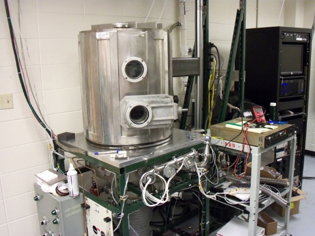
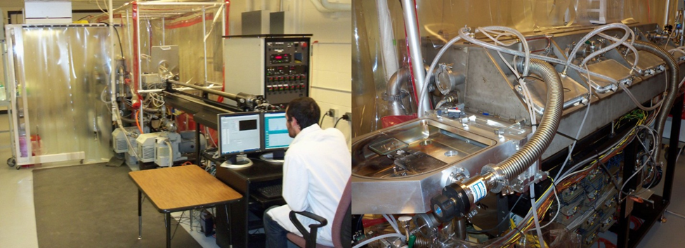 Figure A: CSU Advanced Deposition System will accelerate research and process optimization
The ARDS is in continual use and provides tens of completed substrates and hundreds of individual cells each week for a variety of projects and process-optimization studies. Figure below shows the ARDS system schematic. The magnetic transfer arm can move the substrate to any deposition station for any period of time, allowing for wide process flexibility.
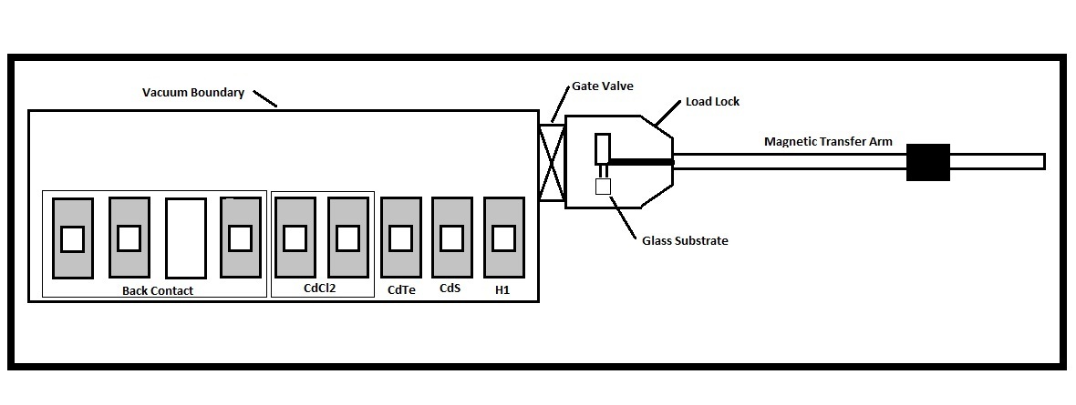 Figure B: Schematic of the Advanced Deposition System (ADS)
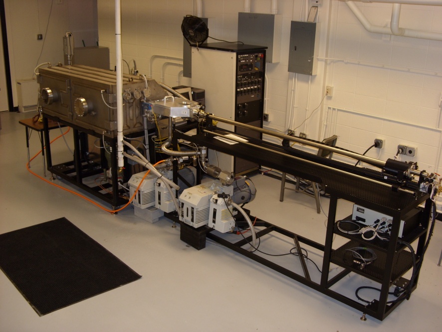
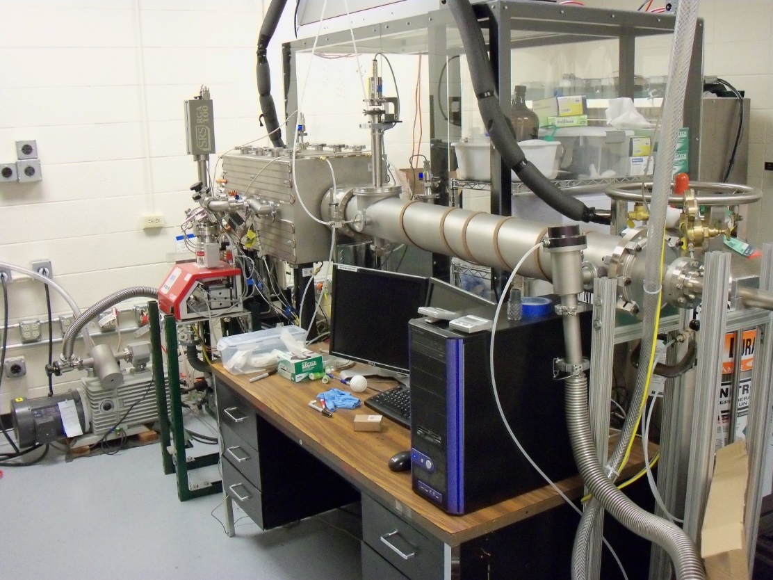
In addition to the ARDS, the NGPV has three other vacuum deposition systems: (i) RF/Pulsed DC deposition system, (ii) thin film deposition by co-sublimation from two sublimation sources, and (iii) plasma deposition system.
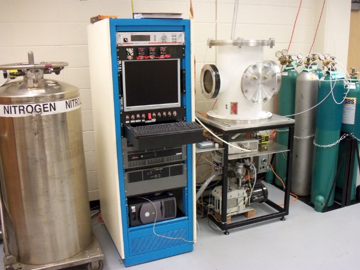
 Plasma Enhancement
These facilities will enable advancing the CdTe PV technology from the current device technology shown in the left in the figure below to the one in the middle and then to the device structure shown on the right.

Figure C: Schematic of current and future advanced device structures (η = cell efficiency)
Many thin film PV processes are thermal processes and some involve flow of gases. A unique capability for large scale thermal, fluids and mechanical modeling has been developed at CSU to model thin film PV processing. The software platform is ANSYS FLUENT and many user defined functions are incorporated to simulate the actual operation of production systems. Two server computers are available for the modeling and industrial scale manufacturing systems processing 120 X 60 cm. modules have been simulated. The agreement between modeling and experimental data is very good. For example, in heat transfer modeling with radiation boundary conditions, the temperature results are within 2% of measured values. In the simulation of industrial scale systems, all the details of the hardware are incorporated (i.e., the geometry is not simplified for modeling) and the material properties as a function of temperature are input into the program.
1. Kephart, J. R. M. Geisthardt; W. S. Sampath, ” Optimization of CdTe thin-film solar cell efficiency using a sputtered, oxygenated CdS window layer” to be published in Progress in Photovoltaics (2014).