The Challenge
From a prior project you already know that any decimal digit
from zero through nine can be displayed by lighting the
appropriate segments of a 7-segment display, as shown in Figure
1.
THE SEVEN-SEGMENT DISPLAY
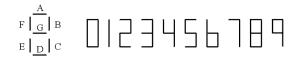
Figure 1: Segment definitions of a 7-segment display.
In Project Six, the design was limited to displaying one BCD
digit on a seven segment display. Project Five resulted in
a multiplier design that produces an 8-bit binary number as the
output. Displaying such numbers in the human readable decimal
format using multiple seven segment display units is thus
essential. Project Seven requires you to design and implement a
circuit to display an 8-bit binary integer using 7-segment
displays using ROM.
With 8-bit inputs however you no longer will be able to
simplify the equations using K-maps; optimization of solution
using algebraic equations in a reasonable time is not possible
either. Therefore, an 8-bit binary to seven-segment
decoder is a good candidate for a ROM based design.
Specifications:
- The input is an 8-bit binary number [I7,...I0] (use switches 0-7 on your DE-2: SW7= I7 (MSB), .... SW0=I0 (LSB).
- Use a 256x24bit ROM. No additional logic gates may be used.
- The output is displayed on three seven-segment display
units. The inputs to the three 7-segment display units, from
left to right, are denoted by [A2,B2, ...G2], [A1, B1, ...G1],
and [A0,B0, ...G0] respectively.
- Use a push-button on DE-2 to manually generate a clock
pulse for reading the ROM.
Figure 2 illustrates the ROM based design. To display all possible 8-bit combinations, three seven segment displays are needed.
For example, when the input binary pattern [I7,....I0] = 1000 0001 is applied, the display should indicate 129, with 1 in the left display, 2 in the middle display and 9 in the right display. Since [I7, ...I0] serves as the address of the ROM, location 1000 0001 of the ROM should contain the 24-bit pattern [X2,G2, F2,E2, D2,C2,B2,A2, X1,G1,F1,E1, D1,C1,B1,A1, X0,G0,F0,E0, D0,C0,B0,A0] corresponding to 129. Since the displays need only 21 bits, and the ROM is 24 bits wide, assume that three bits X2, X1, X0 in the memory are set to 0.
Refer to the DE-2 Manuals regarding how to enable a specific digit on this display. Note: Applying a logic low level to a segment causes it to light up and applying a high level turns it off.
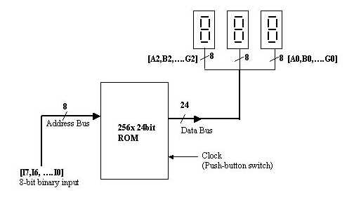
Figure 2: ROM based
design of 8-bit binary to seven-segment decoder
circuit.
- Create or be prepared to create a file containing the contents of the ROM to solve this problem. Rather than entering the binary characters, enter the strings using Hexadecimal.
- Grab the ROM generator here. To use it, follow the instructions in the procedures link below to generate the .mif file. Instead of following the instructions in the procedures link to enter the values into each ROM address individually, open the ROM generator and enter your calculated values into column K. The ROM contents will be generated in the top left portion of the spreadsheet. Copy the ROM contents on the left and paste it into your .mif file.
- Using Quartus-II create the schematic. Following link provides additional information on the procedure to carry out this project.
- Simulate it with input patterns 50 through 75.
- Implement this hardware on your DE-2 Board and test it.
REPORT
Prepare a memorandum which is addressed to the manager of the R&D group at Banana. Go to the Preparing the Memo link to review the general requirements for Banana Memos or to the What to Include and Grading Policy link for the specific things to include in the Project #7 report.
_______________