Digital
System Design (ECE450)
Lab 7
Pulse Clock
and Pyramid Counter (Verilog)
1. Objectives
The objective of this lab is to apply sequential logic design techniques to design and build two different blocks, a clock generator and a pyramid counter.
2. Lab Description and Specs
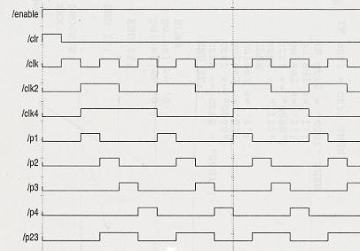
- PULSE CLOCK
The function of this circuit is to take an input clock signal and output the
following signals:
a. clk2: An output clock signal whose period is twice the input clock signal.
b. clk4: An output clock signal whose period is four times the input clock signal.
c. p1, p2, p3 and p4: Four different pulse signals whose pulse width is half the cycle period of the input clock signal and whose period is twice the input clock signal. In addition, the cycle period of these pulse signals are equally divided into four sub-phases (sub-periods) and each sub-phase must be occupied by only one of the four pulses.
d. p23: Another pulse signal whose period is the same as signals p1, p2, p3 and p4, but the width and the location of the pulse are the second and third sub-phases.
The relationship between the input signal and the output
signals is illustrated below. The circuit must also have a clear and an enable
signal.
Illustration:
- PYRAMID COUNTER
Function: A counter that counts from 0 to 15, then pulses a control
signal, pulse1, which reconfigures the counter to count from 0 to 14 (or
1 to 15) and pulses the control signal again, then counts 0 to 13 (or 2 to 15)
and pulses the control signal, etc. When the count goes from 0 to 1 (or 14 to
15) a second control signal, pulse2, is pulsed. The relationship between the
input signal and the output signals is illustrated below.
Illustration:
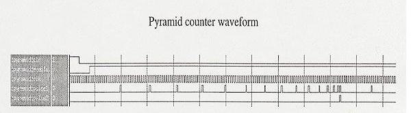
Inputs:
a. Clock Signal
b. Clear Signal
c. An Enable Signal (enables the circuit)
Outputs:
- pulse1
- pulse2
3.
Recommended Procedures
- Pulse Clock:
Use your input clock signal and generate a clock signal with
twice the period. This will be your output, clk2. Draw the truth table
with these two signals as inputs and all the rest of the outputs listed above
as your outputs. Refer to the waveforms for the values of the outputs. From the
truth table you'll see that you can generate all of these outputs with a
minimal amount of combinational logic.
You'll want your enable signal to be synchronous. This means that if
your enable signal becomes active in the middle of a clock period the
circuit is not enabled until the next rising clock edge.
Also implement the design in Verilog and map it to the Altera
FPGA protoboard.
- Pyramid Counter:
There is a very easy way to design this circuit. You are
recommended to use a 4-bit counter. Make the enable signal for this
circuit synchronous also. Build this circuit and do a functional simulation in Cadence.
Write a Verilog model for the pyramid counter and implement and verify it using
the Altera protoboard.
4. Prelab
- truth table for pulse clock
- Verilog code for both pulse clock and pyramid counter. Use case constructs in lieu of "if" statements.
5. Questions
- Describe how you would implement a hierarchical design
in Verilog.