Digital
System Design (ECE450)
Lab
2
Three Bit ALU (Verilog)
1. Objectives
The objective of this lab is to learn the basic logic synthesis steps by synthesizing a 3-bit Arithmetic Logic Unit (ALU) using Verilog.
2. Lab Description and Specs
Function:
Three-bit addition,
subtraction, XOR (bit-wise between A and B), and 3-bit shift-left (on A; shift
in zero at the least significant bit).
Inputs:
fun_sel0 and fun_sel1: Selects
one of the four functions.
ain[2:0]and
bin[2:0]: Bus inputs for the two 3-bit numbers or one 3-bit number.
Outputs:
out[2:0]:
The three-bit number that is the result of the ALU operation.
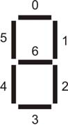
HEX0[6:0] HEX1[6:0]: 2 digits 7-segment display control output to show the final result on 7-segment display.
Here is the 7 segment definition on Altera board, for detail, please refer to the board tutorial.
3. Recommended Procedures
For this lab you will use logic synthesis to design a 3-bit ALU block that performs the four functions on two 3-bit input buses.
- Write a Verilog model for the
3-bit ALU. Use case constructs in lieu of "if" statements.
- Run the Cadence simulator to verify the Verilog model.
- Run Quartus to synthesize it.
- Download it into the Altera Field Programmable Gate
Array (FPGA) protoboard.
- Verify the ALU operations on the protoboard.
- Using 7-segment display to show your final result.
4. Prelab
- Verilog code for 3-bit ALU
5. Questions
- Discuss the advantages of a Hardware Descriptive
Language (HDL).