The
Challenge
You are now ready to tackle
sequential circuits. In this assignment at Banana,
a key subsystem for Banana’s new nano-processor has to be
built. You are to design a
counter, the purpose for which is classified as Banana
Corporation TOP SECRET. As a new engineer
you are expected not to inquire about how this counter will be
used.
Specifications:
You are to build a counter that repeatedly counts with a given
sequence.
Select the sequence from the following list according to your
lab section:
Monday lab section:
0, 9, 11, 12, 13, 7, 6, 5, 14, 2, . .
.
Wednesday lab section: 0,
9, 11, 13, 6, 2, 4, 15, 8, 10, . . .
Thursday lab section:
0, 10, 13,12, 2, 5, 7, 9, 11, 15, . .
.
Part 1: Display the output of the counter on adjacent LEDs of
your choice. Use Key 0 as the clock to the counter.
You may use CLEAR pin, if available, of the flip-flops to
force flip-flops to 0.
Part 2: After you have the counter working in Part 1, the
next step is to display the output of the counter on a seven
segment display.
You designed a Binary to Seven Segment decoder in a previous
lab. Integrate that design and display the output of the counter
on the seven-segment display.
Constraints:
Part 1:
Use D flip-flops in each of your designs. Do not use the
D flip-flops that you build in the previous lab. Use flip-flops
available in Quartus II library. Also note that library devices
are available that contain multiple flip-flops.
Repeat the design using T flip-flops.
Prelab:
Hint:
To use the seven-segment decoder you designed
previously, you need to copy files related to the ROM (lpm_rom0.*)
including the memery content file (Bin_to_BCD.mif) to
your current project directory.
To connect the 4-bit output of your counter to the ROM you have
to convert it to a 8-bit bus as the ROM accept only a bus. Use
the following steps to do so:
Step 1 - First you need to convert your 4-bit output to 8-bits.
Add 4 extra connections and connect them directly to the ground.
These pins will work as the last 4 bits (MSBs).
Step 2 - Draw a bus line from the address input of the ROM.
Step 3 - Name the bus as A[7..0].
Step 4 - Connect individual pins to the bus using wire
connections.
Step 5 - Name the pins using the format A[0], A[1], A[7], where
A[0] is the LSB and A[7] is the MSB. Pins A[0] to A[3] should
come from the counter. You may use a different name but still
keep the last digit as it is.
Figure 1 shows one way to do this where the counter is converted
to a block.
It is possible to build the entire circuit using a single
schematic file. However, it is better to organize the design
into blocks, as the individual blocks can then be reused
for later designs.
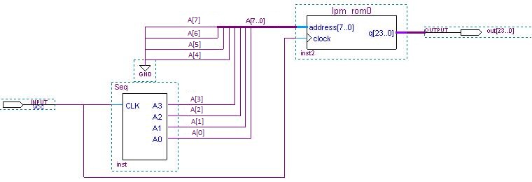
Figure 1 - How to connect wires to bus. Also note the labeling.
REPORT
Prepare a professional memorandum addressed to the manager of the R&D group at Banana. Go to the Preparing the Memo link to review the general requirements for Banana Memos or to the What to Include in Report #10 link for the specific things to include in the Project #10 report.