Project
Number Thirteen:
Verilog Lab
Project Thirteen asks you to design a two way
switch in Verilog and execute the machine instructions. You will
verify your design with a timing diagram simulation and implement
the circuit on your DE board.
The items below will be helpful in competing your project and
preparing your report.
|
This is a bonus lab.
- Successful completion of Lab 13 will
give you an opportunity to earn extra points.
- Provided:
- Your Lab 13
grade satisfies the minimum requirement (i.e.,
>60).
- Bonus
points earned = Your Lab 13 grade/50
- These
bonus points earned will be added to your
final grade.
|
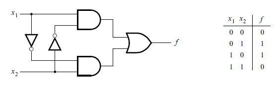
Figure 1: Two way switch circuit diagram and truth table
All the steps will be same for creating and executing a project
in quartus.
Instead of creating a block diagram file to design the circuit, we
will write a Verilog code in a Verilog HDL file.
Table 1 gives symbols for logic operations:
Operation
|
Symbol
|
AND
|
&
|
OR
|
|
|
NOT
|
~
|
Table 1 : Boolean operations and Verilog symbols
Use Table 1 to complete the entries between < > and then
use the following code:
|
module <project_name>(x1,x2,f);
input x1, x2;
output f;
<assign f here>;
endmodule
|
STEPS:
- Compile the Verilog code
- Create the output waveform to crosscheck the given truth table
- Download the code in your DE board and test
No demo.
No prelab.
A report has to be submitted. Please include the following in your
report:
Your report should consist of the following:
- A front page in the
Banana Electronics memo format (check out the Preparing the Memo
).
The text of your 1-page memo should include
- Paragraph 1:
the task in a few sentences 10%;
- Paragraph 2:
say here what you did to get your results given below in
Paragraph 3 10%;
- Paragraph 3:
present your results, referring specifically to Figures 1
and 2, which are attached 10%;
- Paragraph 4:
give a conclusion, stating whether you were successful in
completing the task 10%.
- Overall quality 10%.
- A Verilog code printout
(attached as Figure 1) showing the code 25%, and
- A output waveform
diagram (attached as Figure 2) showing the input and output
signals for all possible input and output combinations 25%.