W. S. Sampath, Professor of Mechanical Engineering
The Mechanical Engineering Department’s Materials Engineering Lab (MEL) under the direction of Professor W.S. Sampath has been in the forefront of CdTe photovoltaic manufacturing technology development since 1991. Numerous pieces of equipment and processes have been developed for synthesis and testing of photovoltaic devices. These include:
- Facilities for measuring film thickness
- Clean room mini-environment for substrate preparation and automated cleaning
- Spray metallization for back electrode formation
- Fabrication facilities for small area device fabrication and analysis
- Accelerated Lifetime Testing (ALT) of devices under automated high illumination and high temperature cycling
- Exposing and testing devices under outdoor conditions emulating sealed modules
- Device characterization including dark JV, light JV, CV, CF, TAS, TID, PHCAP etc. and the capability to perform these as a function of temperature using a cryostat
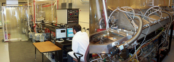
Figure 1. Student fabricating PV devices with the Advanced Deposition System
The recently completed Advanced Deposition System (ADS) (see Figure 1) provides a process-flexible, customizable test bed for producing complete devices on 3 inch by 3 inch or smaller substrates. Completed in August 2010, the system has already produced several hundred unique samples for a variety of research projects and for process optimization. Execution of process sequences is computer-controlled for maximum repeatability and precision using a magnetic transfer arm. The substrate can be moved in any sequence and any combination of process times into 9 different sources. This flexibility provides for rapid process optimization using prototype sources.
The ADS is in continual use and provides tens of completed substrates and hundreds of individual cells each week for a variety of projects and process-optimization studies. Figure 2 shows the ADS system schematic. The magnetic transfer arm can move the substrate to any deposition station for any period of time, allowing for wide process flexibility.
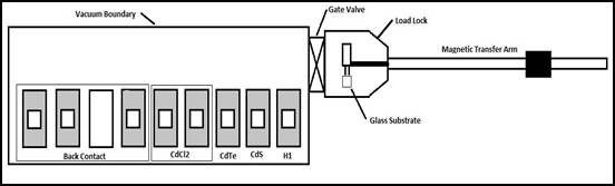 Figure 2 Schematic of the Advanced Deposition System (ADS)
In addition to the ADS, the MEL has three other vacuum deposition systems: (i) RF/Pulsed DC deposition system, (ii) thin film deposition by co-sublimation from two sublimation sources, and (iii) plasma deposition system.
These facilities will enable advancing the CdTe PV technology from the current device technology shown in the left in Figure 3 to the one in the middle and then to the device structure shown on the right. Research to advance the device technology to reach the device structure in the middle in Figure 3 is actively being pursued at CSU with promising results.
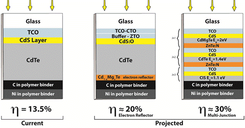 Figure 3: Schematic of current and future advanced device structures (η = cell efficiency)
The laboratory has received funding from the National Science Foundation, Dept. of Energy and Industry. Students design and build PV devices and test them.
For more information, visit their website: http://www.nextgenpv.org/